 Grant Novota
ARM (RISC-V) Computer Processor
Project Overview
The purpose of this project was to implement and simulate a RISC-V processor using a commercial tool from Codasip. The project was completed through 12 phases that lasted about a week each, which were done over the course of a semester at CU Boulder. I had to sign a NDA for this project, so unfortunately I cannot open source my actual code, but I can explain all of the work that went into the creation of my processor model.
The 12 Phases of this project are the following:
- Learn the Codasip environment
- Implement an instruction accurate model of the RISC-V architecture
- Verification and test development
- Schematic for a cycle accurate model of a RISC-V subset (3 instructions)
- Codasip implementation of the RISC-V subset
- Add forwarding to the cycle accurate model and schematic
- Add remaining ALU/branch/jump instructions to the cycle accurate model and schematics
- Add memory operations to the cycle accurate model and schematics
- Add error correcting instructions to the cycle accurate model and schematics
- Add a level 1 cache to the cycle accurate model and schematics
- Implement some performance enhancements
- Project final report
Phase 1: The Codasip Environment
The first phase involved getting introduced to the commercial Codasip tool and its eclipse-based IDE. I learned how to import/export a project and build its various components.
Phase 2: Instruction Accurate RISC-V Model
During this phase I added a basic RV32I instruction set to the instruction accurate hardware model. This model simulated the processor’s behavior on an instruction-by-instruction basis, where each instruction executes completely and updates the register file or memory before the next instruction begins.
Phase 3: Verification & Test Development
This phase involved creating a verification program for the RISC-V instruction set. Here I created an assembly language program to exercise a subset of the instruction set. This process taught one of the critical functions of computer design, which is verifying the design using a test program. The goal of the test program was to detect and report all of the possible errors in a provided flawed hardware design.
Phase 4: RISC-V Subset Schematic
With this phase, I began the creation of a true cycle accurate model of the RISC-V processor and created a schematic of a very simple version of the processor that executes three instructions: add, addi, and halt. The schematic was made up of elements like multiplexors, arithmetic elements, a decoder, control blocks, a register file, and memory. The final version of this schematic can be found under the Phase 8 section, which is the phase where the schematic was completed.
Phase 5: Codasip Subset Implementation
After completing the intial schematic, the next step was to translate it to Codasip code. This involved setting up all of the data signals and registers, designing the instruction decoder, creating the arithmetic logic unit, and building the five different stages of the processor.
Phase 6: Forwarding
Phase 6 added forwarding logic to handle the data hazards. Updates to both the schematic and code were made and there are two types of forwarding which needed to be handled. The first is called data hazard forwarding and handles the RISC-V data hazards, where a register may not be done updating before it’s value is needed by the next instruction in the pipeline. The second hazard is referred to as register file forwarding and is not part of the actual RISC-V design, but is required due to an issue with the Codasip register file implementation. In the Codasip register file model, the write data is written to the register at the end of the clock cycle in the write back stage, which means that if that register is read in the instruction decode stage of the instruction which is three cycles later, the read data will be the old data in the register and the behavior will not match the RISC-V architectural assumptions that the register file is written to during the middle of a clock cycle.
Phase 7: ALU/Branch/Jump Instructions
Next, I finished adding all of the logic that implements the rest of the ALU functions, as well as all of the conditional branch and jump instructions.
Phase 8: Memory Operations
To complete the RISC-V model, the data memory load and store operations were added. This was tricky because a delay needed to be added to the accesses to the data memory and a stall all of the pipeline stages, where data had to be held until the instructions resumed. This logic was created by using a control block that contained a state machine made up of switch statements and counters.
In this stage, the processor schematics were complete:
Phase 9: Error Correcting Instructions
The RISC-V model was completed after phase 8, but in phase 9 I added instructions to simulate how data is encoded/decoded in memory and implemented error correcting code along with this. The encode function took the lower 16 bits of the data selected and computed parity bits, which were necessary to perform single bit correction and double bit detection on the 16 bit data and were appended to the 16 bit data to create a 22 bit data word output. The decode function read the data word (22 bits of info) and performed the error check on it by computing the check bits and the syndrome. If no errors were detected, the lower 16 bits of the input word were written to the output register. If a single error was detected, it was corrected by XORing the bit in error with a 1, the correct 16 bit value was written to the register, and bit 30 of the output word is set to indicate that there was an error. If multiple errors were detected, bit 31 was set to 1. A table of logic was used to figure out how to check for errors.
Phase 10: Cache
In this phase, I created a high level, configurable design for a cache memory system. This included block diagrams of the hardware implementation and state diagrams for the control state machines required. The cache diagrams are shown below:
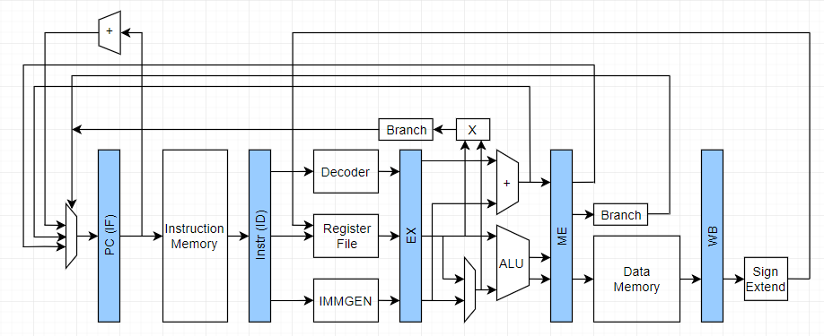
Phase 11: Performace Enhancements
Branch logic was modified in this phase in order to reduce the number of cycles lost to flushing on a taken branch. I added an additional branch function to the design created in phase 8. The picture below shows the high level architecture of the existing RISC-V design. Here, the branch decision is made in the ME stage in all cases, which results in three instructions being flushed on any taken branch or jump.

With some additional hardware, some of the branch instructions can be modified so that only two instructions are flushed on a taken branch. The picture below shows the modification that allows some of the instructions (branch equal/not equal, jump and link, and jump and link register) to have this improvement.
Phase 12: Final Report
The final phase of the project involved writing a final report that summarized the work that was done. This webpage has the same function.
image source: http://images3.programmersought.com/641/35/3550e077d652a2d64c3f716254c6a5c9.JPEG